Thermocouple Board
I wanted to have a simple-to-use board that could interface a thermocouple with a microcontroller, so I created this breakout board for the MAX31856 thermocouple-to-digital IC. The board features I/O buffering as well as protection from reverse voltage, noise, and overcurrent.
Overview
The MAX31856 is specifically designed to work with a large variety of thermocouple types over a broad temperature range, and convert the analog voltage from the junction to a digital temperature value. The chip is relatively expensive for an IC, but cheap compared to pre-built thermocouple devices. It features a SPI interface to communicate and read the temperature value.
Because the MAX31856 operates at 3.3 V, there is a buffer IC to convert voltages as high as 5.5 V to a 3.3 V voltage level. However, if a 3.3 V signal is passed to the buffer IC it will simply be buffered normally with level-shifting. Therefore both 5 V and 3.3 V devices can interface with the thermocouple board. The buffer IC also eliminates noise picked up on the data line or from the microcontroller itself. However, the thermocouple board outputs its result at 3.3 V. While it could relatively easily be modified to output 3.3 V by removing the level-shifting MOSFETs, this original design was intended to work with an Arduino.
Circuit Design
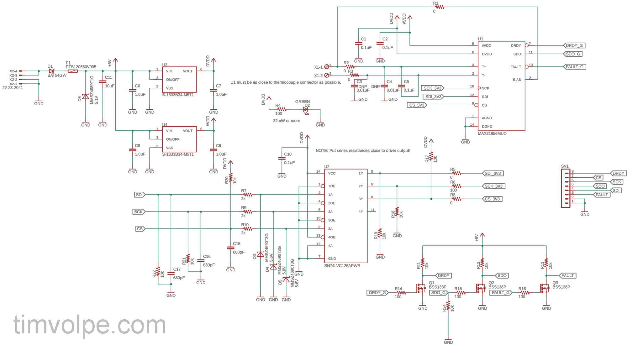
 The Thermocouple Board Circuit
While the MAX31856 is the core of the circuit, there are a large number of discrete components that form the full circuit. The board requires two 3.3 V power rails, an analog and digital rail. This is to separate the digital and analog circuitry and reduce crosstalk from the SPI lines into the tiny differential analog voltage from the thermocouple junction. These rails are supplied by two linear voltage regulators connected to the 5 V input. There is a 5.1 V Zener diode as well as a PTC resettable fuse before the regulators to prevent overcurrent and overvoltage. If the voltage exceeds 5.1 V, the Zener diode will begin to conduct a large amount of current and cause the fuse to open. If there is a short and a large amount of current is pulled from the 5 V input, then the fuse will also open. The PTC resettable fuse should theoretically reset after the condition has been cleared and allowed to cool down. A Schottky diode is also present on the 5 V input to prevent reverse voltage at the expense of a slight voltage drop.
The SPI data lines, SDI, SCK, and CS, are connected to an SN74LVC1G17 buffer and level-shifter. The IC can handle inputs up to 6.5 V, but a 5.5 V Zener diode is present on each input to prevent the voltage from getting too high. These inputs have 2k resistors to reduce the current draw in an overvoltage condition. This works because the buffer IC draws very little current and the SPI communication is relatively slow, so the input lines can have a larger resistance. There are also parallel RC circuits on each line to short noise to ground. The CS input is pulled up, while the others are pulled down to establish a default state.
The output of the buffer IC is connected directly to the MAX31856. The thermocouple signal enters through the pair through a pair of screw terminals, and is connected to the MAX31856 in a manner specified by the datasheet. The connection to the chip is a differential pair, meaning the length of both traces is identical and they are routed similarly. This is to give them the same parasitic characteristics. The resistance should be same, and the capacitance and inductance should be similar if they are routed close together in the same path. The datasheet suggests series resistors as well as capacitors two ground and a differential capacitor connecting before lines in order to reduce noise. The value of these components depends on the measured performance and noise in the final circuit. I found that without the capacitors, the device was not able to measure temperature correctly due to noise.
The output of the MAX31856 is connected to three MOSFETs which shift the digital signal back up to 5 V. These are inherently protected from reverse voltage by the MOSFETs themselves. A gate resistor was added which can be adjusted to reduce overshoot of the gate voltage. The MAX chip outputs SDO, DRDY and FAULT. DRDY defines if a measurement conversion is complete, while FAULT indicates a thermocouple fault. Both of these are used to determine the state of the MAX chip.
PCB Design
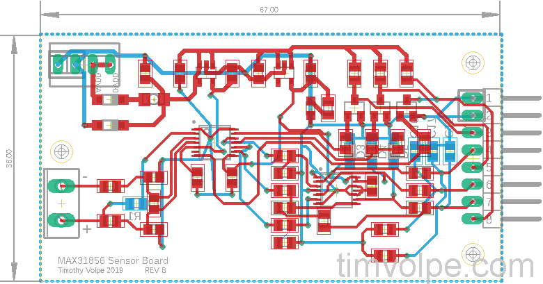
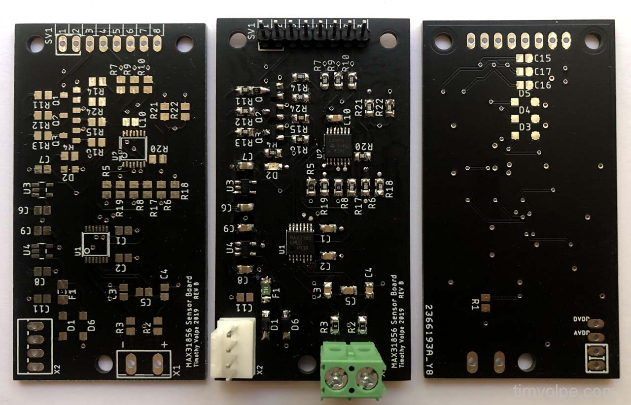
The PCB was design with all surface-mount components except for the connectors. The first revision of the circuit, REV A, had some issues such as the lack of some noise filtration, the chosen MOSFETs not operating properly, and a few routing issues. The second revision, REV B, fixed all these issues. The only mistake was accidently deleting the connection between one of the MOSFETs and the source resistor, which was easily fixed by bridging with a 0 Ohm jumper. Mounting holes were also added.
The PCB was designed in Eagle and manufacture red by JLCPCB.
 The Thermocouple Board PCB Design
 The Final Manufactured PCB
Usage
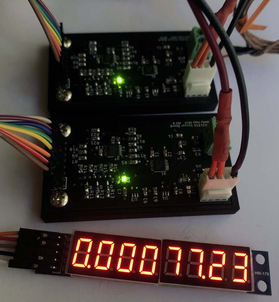
The device can be used for an endless array of projects due to its flexibility. As a proof of concept, I devised a simple prototype using an ATmega128 and two of the thermocouple boards.
 Two Thermocouple Boards Working in Tandem. Only One Thermocouple is Present.
I connected a pre-built array of 7 segment displays which are used to show the measured temperature for each. I currently only have one thermocouple so only one temperature can be displayed at a time.
The ATmega128, not pictured, is soldered to a breadboard with a 16.0 MHz oscillator and appropriate connectors. A USBasp is used to power and program the assembly.
Conclusion
Communication with the device can be done with any SPI-capable microcontroller. The SPI command structure is available in the MAX31856 datasheet. I used an Arduino to test the device and was able to perform both continuous and single temperature measurements with a K-type thermocouple. However, K-, J-, N-, R-, S-, T-, E-, and B-type thermocouples are supported.

